
Comparison of profile with solid SiO2 and porous SiO2
Computational conditions
- The width and the thickness of resist are 50[nm] and 70[nm], respectively. The thickness of Si of substrate bottom is 50[nm].
- Etching by Fluorocarbon plasma
- 34 reactions including generation of comlexes and polymers, ion assist etching are used.
- SiO2CxFy is the precursor to etching.
- Average and Standard deviation of pore of porous SiO2 are 6[nm] and 2[nm], respectively. Occupancy ratio of pore is 40%.
Result
-

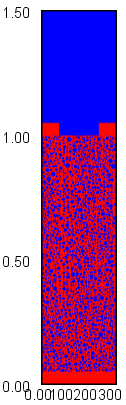
Solid SiO2 initial pforile
-
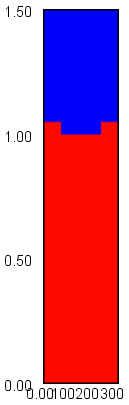
Porous SiO2 initial profile
-
![Polymer layer at 10[s]](http://www.psinc.co.jp/english/assets_c/2015/06/solid_polymer_T%3D30-thumb-131x404-466.gif)
Polymer layer at 10[s]
-
![Polymer layer at 20[s]](http://www.psinc.co.jp/english/assets_c/2015/06/solid_polymer_T%3D20-thumb-130x404-465.gif)
Polymer layer at 20[s]
-
Polymer layer at 30[s]
-
![Solid layer at 10[s]](http://www.psinc.co.jp/english/assets_c/2015/06/solid_prof_T%3D10-thumb-132x405-467.gif)
Solid layer at 10[s]
-
![Solid layer at 20[s]](http://www.psinc.co.jp/english/assets_c/2015/06/solid_prof_T%3D20-thumb-132x404-468.gif)
Solid layer at 20[s]
-
![Solid layer at 30[s]](http://www.psinc.co.jp/english/assets_c/2015/06/solid_prof_T%3D30-thumb-131x404-469.gif)
Solid layer at 30[s]
-
![Polymer layer at 10[s]](http://www.psinc.co.jp/english/assets_c/2015/09/porus_polymer_T%3D10-thumb-131x407-564.gif)
Polymer layer at 10[s]
-
![Polymer layer at 20[s]](http://www.psinc.co.jp/english/assets_c/2015/09/porus_polymer_T%3D20-thumb-130x405-565.gif)
Polymer layer at 20[s]
-
![Polymer layer at 30[s]](http://www.psinc.co.jp/english/assets_c/2015/09/porus_polymer_T%3D30-thumb-132x404-566.gif)
Polymer layer at 30[s]
-
![Porous layer at 10[s]](http://www.psinc.co.jp/english/assets_c/2015/09/porus_prof_T%3D10-thumb-130x405-567.gif)
Porous layer at 10[s]
-
![Porous layer at 20[s]](http://www.psinc.co.jp/english/assets_c/2015/09/porus_prof_T%3D20-thumb-130x407-568.gif)
Porous layer at 20[s]
-
![Porous layer at 30[s]](http://www.psinc.co.jp/english/assets_c/2015/09/porus_prof_T%3D30-thumb-130x406-569.gif)
Porous layer at 30[s]

![Polymer layer at 10[s]](http://www.psinc.co.jp/english/assets/img/solid_polymer_T%3D30.gif)
![Polymer layer at 20[s]](http://www.psinc.co.jp/english/assets/img/solid_polymer_T%3D20.gif)
![Solid layer at 10[s]](http://www.psinc.co.jp/english/assets/img/solid_prof_T%3D10.gif)
![Solid layer at 20[s]](http://www.psinc.co.jp/english/assets/img/solid_prof_T%3D20.gif)
![Solid layer at 30[s]](http://www.psinc.co.jp/english/assets/img/solid_prof_T%3D30.gif)
![Polymer layer at 10[s]](http://www.psinc.co.jp/english/assets/img/porus_polymer_T%3D10.gif)
![Polymer layer at 20[s]](http://www.psinc.co.jp/english/assets/img/porus_polymer_T%3D20.gif)
![Polymer layer at 30[s]](http://www.psinc.co.jp/english/assets/img/porus_polymer_T%3D30.gif)
![Porous layer at 10[s]](http://www.psinc.co.jp/english/assets/img/porus_prof_T%3D10.gif)
![Porous layer at 20[s]](http://www.psinc.co.jp/english/assets/img/porus_prof_T%3D20.gif)
![Porous layer at 30[s]](http://www.psinc.co.jp/english/assets/img/porus_prof_T%3D30.gif)