
Si etching by Ar/Cl2 plasma and comparison with FPSM2D
Computational conditions
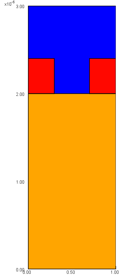
- The width,thickness of resist and thickness of Si substrate are 0.3[um],0.4[um] and 2[um],respectively in FPSM2D.
- The diameter of hole is 0.4[um] in hole etching by FPSM3D(1/2 model to z direction).
- The width and length of trench are 0.4[um] and 0.2[um], respectively in trench etching by FPSM3D(1/2 model to z direction). the thickness of resist and SI substrate are same as above.
- The reflection model of incident ions on the resist depend on the incident angle and energy. But no physical and chemical reactions between radicals,ions and the resist are assumed.
- The 17 kinds of physical/chemical reactions including ion assist etching between Si substrate and incident particles are considered.
- Ion and radical information, number of reactive kinds ans reaction probabilities are same in all simulations.
Result
-

FPSM2D initial profile
-
![FPSM2D result at 900[s]. The etch rate is about 90[nm/min]](http://www.psinc.co.jp/english/assets_c/2015/09/fpsm2d_T%3D900-thumb-300xauto-571.gif)
FPSM2D result at 900[s]. The etch rate is about 90[nm/min]
-
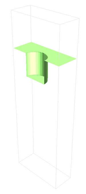
FPSM3D hole initail profile
-
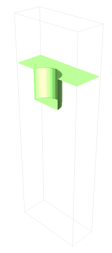
![FPSM3D hole at 300[s]](http://www.psinc.co.jp/english/assets_c/2015/09/hole_T%3D300-thumb-300xauto-573.gif)
FPSM3D hole at 300[s]
-
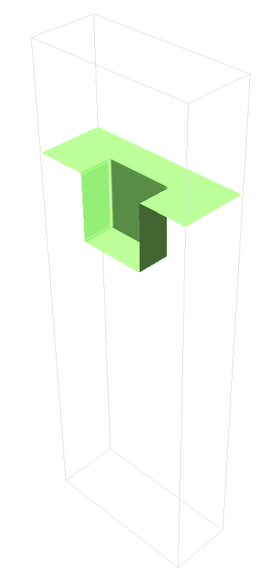
![FPSM3D hole at 900[s]](http://www.psinc.co.jp/english/assets_c/2015/09/hole_T%3D900-thumb-300xauto-574.gif)
FPSM3D hole at 900[s]
-

FPSM3D trench initial profile
-
![FPSM3D trench at 300[s]](http://www.psinc.co.jp/english/assets_c/2015/09/trench_T%3D300-thumb-300xauto-576.gif)
FPSM3D trench at 300[s]
-
![FPSM3D trench at 900[s]](http://www.psinc.co.jp/english/assets_c/2015/09/trench_T%3D900-thumb-300xauto-577.gif)
FPSM3D trench at 900[s]
![FPSM2D result at 900[s]. The etch rate is about 90[nm/min]](http://www.psinc.co.jp/english/assets/img/fpsm2d_T%3D900.gif)
![FPSM3D hole at 300[s]](http://www.psinc.co.jp/english/assets/img/hole_T%3D300.gif)
![FPSM3D hole at 900[s]](http://www.psinc.co.jp/english/assets/img/hole_T%3D900.gif)
![FPSM3D trench at 300[s]](http://www.psinc.co.jp/english/assets/img/trench_T%3D300.gif)
![FPSM3D trench at 900[s]](http://www.psinc.co.jp/english/assets/img/trench_T%3D900.gif)